Introduction: New Manufacturing Paradigm for Electronics Manufacturing
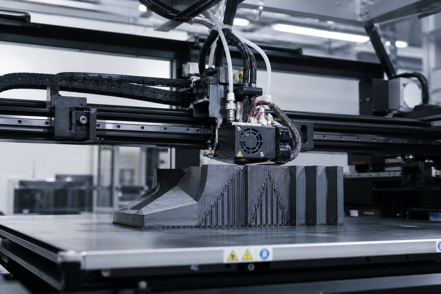
The electronics manufacturing industry is undergoing a profound change. With the shortening of the life cycle of consumer electronics products, the growth of personalized needs and the strengthening of miniaturization trends, traditional manufacturing processes are facing increasing challenges. 3D printing technology is opening up new possibilities for electronics manufacturing with its rapid prototyping, high flexibility and complex structure manufacturing capabilities. From PCB rapid prototyping to customization of end product casings, 3D printing is reshaping the design, development and production processes of electronic products.
PCB rapid prototyping
Printed circuit board (PCB) is the core component of electronic products. The traditional PCB manufacturing process is complex, long cycle and high cost, especially not suitable for the needs of small batches and rapid iteration. 3D printing technology provides a revolutionary solution for PCB prototyping. By using alternating printing of conductive ink and insulating materials, multi-layer PCB prototypes can be directly manufactured, significantly shortening the development cycle. In addition, 3D printing can also realize special-shaped PCB design that is difficult to achieve with traditional processes, providing more freedom for product innovation.
Personalized customization of electronic enclosures
The casing of electronic products not only plays a protective role, but is also an important carrier of the product's brand image. The traditional injection molding process requires expensive molds and is not suitable for small batch and personalized production. 3D printing technology can realize rapid customization of housings at extremely low cost. Whether it is complex heat dissipation structure, ergonomic design, or the integration of brand logo, 3D printing can easily realize it. For small-volume production of professional electronic equipment, medical equipment, industrial controllers, etc., 3D printed housings have significant cost and time advantages.
Optimal design of heat dissipation structure
Heat dissipation is a key challenge in electronic product design. With the improvement of chip performance and miniaturization of equipment, heat dissipation issues have become increasingly prominent. 3D printing technology provides unprecedented design freedom for heat dissipation structure optimization. Through topology optimization algorithms, complex heat dissipation structures that cannot be manufactured by traditional processes can be designed, such as bionic heat dissipation fins, internal flow channels, gradient pore structures, etc. These optimized designs can significantly improve heat dissipation efficiency, reduce equipment operating temperature, and extend service life.
Innovative solutions for electromagnetic shielding
Electromagnetic compatibility (EMC) is an important certification that electronic products must pass. Traditional electromagnetic shielding methods mainly rely on metal shells or conductive coatings, which are heavy and costly. 3D printing technology provides new solutions for electromagnetic shielding. By adding conductive fillers (such as copper powder, silver powder, carbon nanotubes, etc.) to the printing material, components with electromagnetic shielding functions can be directly printed. In addition, periodic structures (such as electromagnetic band gap structures) with specific frequency response characteristics can also be designed to achieve selective electromagnetic shielding.
Flexible electronics and wearable devices
Flexible electronics and wearable devices are important development directions in the electronics industry. 3D printing technology is particularly suitable for the manufacturing of flexible electronics. By alternating printing with flexible and conductive materials, bendable and stretchable circuit structures can be created. This technology is particularly suitable for manufacturing smart clothing, flexible sensors, medical monitoring equipment and other products. In addition, 3D printing can also achieve integrated manufacturing of electronic components and structures, reduce assembly processes, and improve product reliability.
Micro-nano scale 3D printing
As electronic products develop towards miniaturization, micro-nano-scale 3D printing technology is becoming more and more important. Two-Photon Polymerization (TPP) technology can achieve sub-micron level resolution and is suitable for manufacturing precision devices such as micro-optical components, microfluidic chips, and micro-sensors. This technology provides new manufacturing methods for the miniaturization and integration of electronic products.
Material selection and process optimization
Electronic manufacturing has special requirements for materials, including insulation, thermal conductivity, flame retardancy, dimensional stability, etc. Materials currently available for 3D printing in electronic manufacturing include engineering plastics (such as ABS, PC, PEI), high-performance polymers (such as PEEK, LCP), conductive materials (such as conductive ABS, copper-based composite materials), etc. In terms of process optimization, it is necessary to focus on dimensional accuracy control, surface quality improvement and post-processing processes (such as metallization, spraying, welding, etc.).
Quality control and reliability testing
The quality of electronic products is directly related to product performance and safety. 3D printed electronic products require the establishment of a complete quality control system. Including raw material inspection, process parameter monitoring, dimensional accuracy testing, electrical performance testing, environmental reliability testing (such as high and low temperature cycles, damp and heat testing, vibration testing, etc.). Especially for critical applications (such as medical, automotive, aerospace), relevant industry standards and certifications are also required.
Future Outlook
The application prospects of 3D printing in electronic manufacturing are very broad. With the advancement of material technology, improvement of printing accuracy and reduction of costs, 3D printing will gradually transition from the current prototype manufacturing and small batch production to mass production. In the future, we may see smartphones, wearable devices, smart home products, etc. completely manufactured by 3D printing. At the same time, cutting-edge technologies such as 4D printing (programmable materials), nano-3D printing, and bioelectronic 3D printing will also bring more possibilities to the electronics manufacturing industry.
Conclusion
3D printing is profoundly changing the landscape of electronics manufacturing. From PCB rapid prototyping to customization of end product casings, from heat dissipation structure optimization to electromagnetic shielding innovation, 3D printing provides unprecedented freedom for electronic product design and manufacturing. Electronic manufacturing companies should actively embrace this technological change, explore application scenarios suitable for their own business, and enhance innovation capabilities and market competitiveness. As technology continues to mature, 3D printing will play an increasingly important role in the electronics manufacturing industry.
Submit a model, drawing, image or written notes. Engineers will review material, process, finishing and delivery based on actual use.